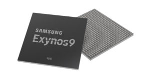
Samsung has now shared its new roadmap for the upcoming chipset today. As per the source, Samsung is now planning to introduce the 7nm LPP, 5LPE (5nm Low Power Early), 4LPE/LPP (4nm Low Power Early/Plus) and 3GAAE/GAAP (3nm Gate-All-Around Early/Plus) process technologies.
Samsung new 7nm LPP process will be built using new EUV lithography solution and will be ready by the second half of this year and will enter mass-production by the first half of 2019. Samsung biggest competitor TSMC has already moved ahead with the 7nm chipset for Apple which will also use EUV Lithography solution and has already started working on 5nm based chipset by the first half of 2019.
Whereas Samsung is going to start production of the 5nm LPE process which has ultra-low power consumption by 2019. After that, Samsung will begin working on 4nm LPP process by 2020 and would be the last chipset to use the FinFET process with smaller cell size and improved performance.
Finally, Samsung will start working on 3nm node process based on own GAA architecture MBCFET (multi-bridge-channel FET). The 3nm node chipset will not enter production not earlier than 2022.


